COFFE Overview
COFFE Configuration File Parameter Descriptions
All FPGA architecture related parameters are stored under the namespace “fpga_arch_params”
The following section will describe each parameter in the input yaml file and one can look to the provided example file to determine the corresponding datatype for each param.
Utility Parameters
Parameter |
Description |
|---|---|
arch_out_folder |
The directory in which output files will be stored. If not specified, the directory containing this file is used as output dir. |
area_scale_factor |
Standard cell to custom area scaling factor |
freq_scale_factor |
Standard cell to custom frequency scaling factor |
power_scale_factor |
Standard cell to custom power scaling factor |
The above scaling factors can be useful when one doesn’t have access to a modern standard cell library but does have access to a more modern spice deck (or vice versa)
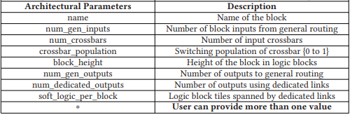
FPGA Architecture Parameters

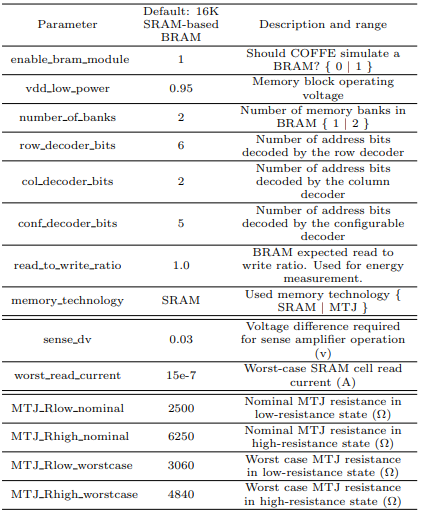
Memory Block Parameters
Memory block parameters are used if one wants to model the FPGA BRAM.
Additional Tx Sizing (Custom Circuit Flow) Parameters
Parameter |
Description |
|---|---|
transistor_type |
Can use “bulk” or “finfet” transistor |
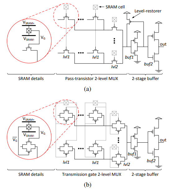
switch_type |
Uses either “pass_transistor” or “transmission gate” in FPGA MUX/LUT circuitry. |
vdd |
FPGA supply voltage |
vsram |
Voltage of FPGA configuration SRAM cells (Importantly also the boost voltage for pass transistors) |
vsram_n |
SRAM cells VSS |
gate_length |
Gate length (in nm) of minimum size transistor |
rest_length_factor |
Factor which determines gate length of the level-restorer transistor in Figure 1a. length will be equal to “rest_length_factor” x “gate_length” |
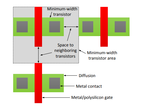
min_tran_width |
Minimum transistor diffusion width (nm) |
min_width_tran_area |
Minimum-width transistor area (nm^2) |
sram_cell_area |
Area of a single SRAM cell in number of “min_width_tran_area” |
model_path |
Path to SPICE device model files |
model_library |
Library in model file to use |
metal |
List of metal layer RC values to use, the following rows in this table represent different metal layers |
metal[0] |
All wires except the general routing wires are implemented in this layer. |
metal[1] |
General routing wires will be implemented in this layer |
metal[2] |
Memory array wires will be implemented in this layer |
metal[3] |
This layer is used in MTJ wordline (if BRAM technology is MTJ) |
The below figures may help with understanding some of the above parameters and how they relate to the FPGA architecture.
Hardblock Parameters